



Special Topic on Ferroelectric Memory, Storage, and Compute for AI Systems: Devices, Integration, and Silicon Demonstrations
Guest Editors
Editor-in-Chief
Aim and Scope
Artificial intelligence has made memory the binding constraint on computing. Capacity, bandwidth, and energy per bit now govern what can be trained and served, and the cost of moving and holding data increasingly dominates the cost of the arithmetic itself. Ferroelectrics offer a potential solution. Their combination of switchable polarization, non-volatile retention, and low-energy switching addresses storage density, standby power, and data movement at once, and the fluorite-structure hafnia and zirconia systems have brought that capability into the CMOS foundry rather than leaving it in the laboratory. This Special Topic builds its foundation on the 2025 JxCDC Special Topic on ferroelectric information processing and storage. It focuses on ferroelectrics for memory, storage, and in-memory computing in mainstream AI and general-purpose computing, across three deployment settings that impose sharply different constraints: AI data centers, physical / embodied AI, and automotive platforms. Above all, it prioritizes silicon: fabricated, measured demonstrations — test chips, integrated IP, and prototype systems that have been through a foundry or PDK-supported flow — and quantitative benchmarking against the incumbents they aim to displace. Contributions are expected to report the figures of merit that determine whether a ferroelectric technology could disrupt existing state-of-the-art technologies or offer new solutions for existing architectures. Beyond regular contributions, perspectives and industrial roadmap papers are especially welcome.
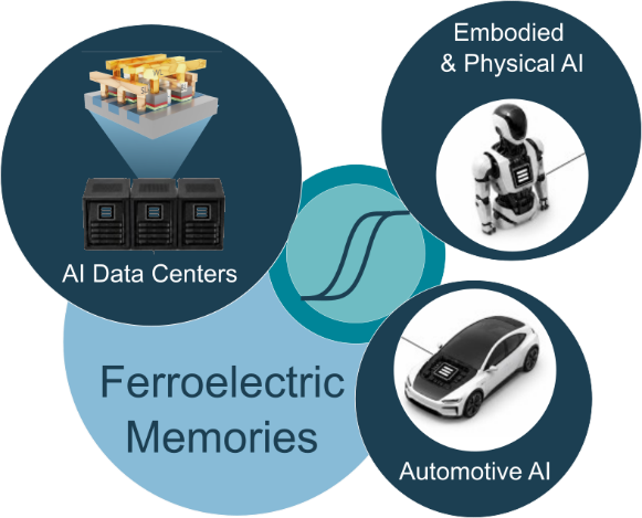
We solicit work on ferroelectric technologies spanning materials, devices, CMOS integration, circuits, and architectures across the applications above, with an emphasis on quantitative energy-efficiency metrics and performance benchmarks against incumbent technologies.
- AI data centers. Data-center AI demands the highest performance, – bandwidth, capacity, and throughput per rack -as the cost of moving and holding weights, KV-cache, and checkpoints comes to dominate training and inference at scale. Ferroelectric memory addresses this with density, energy efficiency, and non-volatility across high-density storage, DRAM-alternative and CXL-tier candidates, 3D FeNAND toward the thousand-layer regime, and charge-domain in-memory compute, with cryogenic operation a further route to performance per watt.
- Physical and embodied AI. Robots, drones, aviation, and industrial edge platforms demand the lowest possible power — running inference within hard thermal and form-factor limits, often without connectivity, so every picojoule counts. Non-volatile ferroelectric memory and in-memory compute address this by holding weights through power cycling, waking instant-on, and keeping energy per inference low for battery- and harvest-constrained nodes, while tolerating shock, vibration, and temperature swings.
- Automotive AI. Automotive AI demands reliability above all — inference hardware and non-volatile memory that hold automotive-grade performance across the full temperature range and qualification-grade lifetimes. Ferroelectric memory must therefore meet these conditions, with retention, endurance, and imprint treated as first-order design constraints.
Topics of Interest
We welcome contributions in the following areas:
- Silicon demonstrations and tape-outs. Measured test chips, integrated ferroelectric IP, and prototype systems from a foundry or PDK-supported flow, across all domains above.
- Materials and devices. Hafnia and zirconia, wurtzite nitrides, and antiferroelectrics, and the FeFET, capacitor, and array-level devices built on them.
- CMOS integration and process technology. Front-end, back-end-of-line, and monolithic-3D integration, thermal budget compatibility, and foundry and PDK support.
- Reliability and characterization. Endurance, retention, imprint, wake-up, fatigue, and variability, with failure analysis and array-level statistics across the relevant temperature and radiation conditions.
- Modeling and simulation. Compact and behavioral models, PDK-grade parameter extraction, electrothermal co-simulation, and multiscale modeling, ideally validated against measured silicon.
- Circuits, architecture, and systems. Memory, in-memory, and mixed-signal circuit design, array and system architectures, and heterogeneous integration and packaging.
- Benchmarking and co-design. Design- and system-technology co-optimization (DTCO/STCO) and quantitative power-performance-area benchmarking against CMOS incumbents.
Submission Guidelines
Submit your paper through the JXCDC submission site.
Deadlines
- Open for Submission: September 2, 2026
- Submission Deadline: November 15, 2026
- First Notification: December 1, 2026
- Revision Submission: December 15, 2026
- Final Decision: January 5, 2027
- Online Special Topic Publication: February 1, 2027
Papers submitted earlier than the submission deadline will be reviewed upon submission and if accepted will get published earlier than the timeline listed above.